- News
- City News
- bhopal News
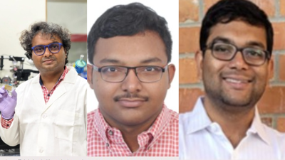
- IISER Bhopal researchers develop tech to support low-cost chip production
Trending
IISER Bhopal researchers develop tech to support low-cost chip production
End of Article
Follow Us On Social Media

Hot Picks
Top Trending
Tired of too many ads?go ad free now
Trending Stories
In City
Entire Website
- Delhi launches Rs 160-crore underground cabling project in Chandni Chowk
- Watch: Strong earthquake rattles Kolkata, residents flee homes, offices in panic
- Bengaluru–Hyderabad rail journey set to get faster from next month
- FIR against 6 directors of 2 realty firms for s 5cr fraud in Gurgaon
- Delhi’s 61-km road along with Najafgarh drain corridor to ease traffic and boost connectivity
- A ‘helping’ hand in fake ED raid at retired employer's house and how plot unravelled
- City gets 2 new auto routes to facilitate last-mile connectivity
- Gold jewellery worth Rs 1 crore stolen from house in Bengaluru
- Elevated Metro link to Kondhwa-Yewalewadi likely to be ready by 2030-31: Officials
- Kejriwal, Sisodia Acquittal: Delhi court cites lack of evidence; CBI to file appeal
- T20 World Cup Live: Lifeline for Pakistan as England beat NZ to top Super 8 group
- England national cricket team vs New Zealand national cricket team match Live Scorecard: NZ win toss, opt to bat in Colombo
- India GDP Q3 Growth Data 2026 Live Updates: First GDP data under new series to be released today
- Earthquake jolts Kolkata, panic among residents
- CBSE Class 10 Science Paper 2026 PDF Now Available: Download and Analyze
- Why is stock market down today? Nifty50 falls 317 points, BSE Sensex crashes 961 points to close at 81,287- top reasons
- Kejriwal, Sisodia Discharged: Delhi court finds no evidence of conspiracy; CBI plans to appeal
- Delhi Liquor Policy Case News Live Updates: 'I'll quit politics if BJP wins even 10 seats,' Kejriwal dares PM Modi to hold fresh Delhi polls
- “Be optimistic about the future,” advises Elon Musk to youth: Can Gen Z afford that mindset in 2026?
- We drove 2,000 km in an EV across Maharashtra: The highway was effortless, the charging wasn’t
Tired of too many ads?go ad free now


Explore Every Corner
Across The Globe
Matthew TkachukDelhi Excise Policy CaseDon SweeneyAntoine Dupont Net WorthUEFA Champions LeagueWilliam NylanderOlympic medalist Chloe KimStellaron Hunter Blade FortniteDylan LarkinT20 World Cup Points TableToronto Maple LeafsNFL Trade NewsStephen CurryJohn CenaKai TrumpNFL Trade NewsResident Evil RequiemLauren KyleIndia Qualification ScenarioCBSE Class 10 Science PaperStock Market todayIND W vs AUS W Live ScoreUttarakhand Gang RapePakistan F16Umran AkmalSourav GangulyWBCSC Assistant Professor RecruitmentR AshwinT20 World CupT20 World Cup 2026 Schedule
Hot on the Web
The Kerala Story 2R MadhavanThaai KizhaviVivek OberoiKeanu Reeves QuoteRashmika MandannaAjith Kumar HouseChiranjeeviRashmika Mandanna Sangeet CeremonyJana NayaganVijay Deverakonda Wedding AlbumAnkita LokhandeYami GautamSindhutai SapkalSai Pallavi HouseSunil Bharti MittalKamal BungalowHair Growth OilsNamo Bharat Rrts Corridor'O'Romeo' Box Office CollectionMumbai AirportRashmika- Vijay Wedding PicturesLunar Eclipse City Wise TimingsFlorida ParkKuno National ParkHoroscope TodayThe 50The Bluff Movie ReviewBorder 2 Movie ReviewTu Yaa Main Movie ReviewToday Gold Rate in ChennaiDelhi Weather TodayDelhi AQI TodayMumbai AQI TodayMaharashtra Public Holidays 2026Anthropic Ceo Dario AmodeiVivo V70Suryakumar Yadav Luxury ApartmentWarner BrosQuote Of The Day By Louis PasteurNarayana Murthy AI Warning
Trending Topics
Luke HumphriesENG vs NZ LiveAiden MarkramGavin TuckerAustin ReavesResident Evil RequiemThe Kerala Story 2Drew McIntyreArvind KejriwalTony DungyToronto Maple LeafsDaniel ZellhuberBig 12 Mens Basketball TournamentDylan LarkinIGNOUFrancisco CerundoloHarrison SmithBrady TkachukRobert VadraMark CarneyPOCSO CaseSSC CHSL Result 2026Bill ArmstrongSourav GangulyUS Stocks TodayLewis HamiltonOlympic Gold Medalist Quinn HughesGurdaspur encounterOdisha farmerSharad PawarDeadliest Female AnimalsTriumph 350ccUpcoming Cars In MarchSam AltmanPlaystation Plus Monthly GamesNano Banana 2Patna Gol GharMeta Chip Deal With GoogleKuwait Military ServiceHow to watch ICC T20 World Cup 2026 in USAHow to watch ICC T20 World Cup 2026 in CanadaHow to watch T20 World Cup online in India
Popular Categories
HeadlinesSports NewsBusiness NewsIndia NewsWorld NewsBollywood NewsHealth+ TipsIndian TV ShowsTechnologyTravelEtimesHealth & FitnessHow to watch T20 World Cup OnlineIndia vs Pakistan MatchAstrologyAutoWeather TodayGold Rate Today DelhiSilver Rate TodayPlatinum Rate TodayIs Bank open todayMarch Bank HolidaysMarch Public HolidaysDeorhiTechnology NewsInternational SportsPublic HolidaysBank HolidaysT20 World Cup Squad IndiaT20 Wprld Cup Squad
Trending Videos
Preventing Heart Disease: Small Steps, Big ImpactGen Z & Gen Alpha: Building Heart Health EarlyLife After a Heart Attack: The Road to Stronger RecoveryWomen & Heart Health: Beyond the ObviousPak-Afghan War: Security Expert Say Conflict Could End Badly for IslambadGOP Plan ‘Backfires’, Clinton Deposition Sets TRAP; Trump To Testify In Epstein Probe Next?Kanpur: Food & Drug Seizures, Codeine Racket Bust, Security Cams Plan & MoreExperts Answer Who Is Really Running Pakistan’s Afghan Policy?Akshay Kumar, Rajpal Yadav & Team Promote Bhooth BanglaAsaduddin Owaisi Slams Gujarat Marriage Law, Calls It Against Right To PrivacyAhmedabad: Infra Push, Campus Case, Market Cooldown & MorePakistan Army Blames India Again For 'Open War' Against Afghanistan, Calls Taliban Delhi’s Proxy
Latest News
Horoscope Today: Daily astrological predictions for February 28, 2026Literature that preserves its cultural authenticity resonates with readers: Banu MushtaqCuttack to celebrate its iconic dish, ‘dahibara aludam’, on March 1Sun, spa & sisterhood: Why Bali is the ultimate destination for all girls’ escapeRajgir Zoo Safari to remain shut on March 3 and 4 for HoliNagaland inks MoU with IMD to boost weather forecastingBihar assembly Speaker reviews tap water scheme with MLAs, officialsAfter IPS officer’s arrest bid, govt grants safeguards to police under BNSSSanthal Pargana Municipal Polls: BJP Faces Setbacks, Independents and Rebels TriumphJharkhand ULB Election Results 2024: Counting Underway for 48 Urban Local BodiesNagaland dy CM condemns attack on NE womenBihar govt steps up efforts to revive Sasamusa sugar mill in GopalganjGumla & Lohardaga Ward Councillor Elections: Incumbents Re-elected, Strong Public MandateLiquor, ganja consumption rampant in airport parking areas; director writes to policeRajpal Yadav on launching his digital universe: Everything is at your fingertipsNirmala secures chairperson’s post of Phusro civic bodyNFL Rumors: Patriots set to pair Stefon Diggs and A.J. Brown with Drake MayeSeven special teams to inspect city drains
Copyright © 2026 Bennett, Coleman & Co. Ltd. All rights reserved. For reprint rights: Times Syndication Service